I’ve made a fair number of PCBs. A lot of them have not been great, but many have worked including my MacSAO last year (after a couple of bad designs) and the StarSensor this year looks good too. I try to be adventurous enough to try new things when I do this. The keyboard driver on my PiBook for instance, was the first time I’d ever done a 4-layer board.
The board is the first time I’ve ever utilized full-color-printing on a board offered by a couple of board houses. Historically, I’ve always almost always gone with JLCPCB. They make a decent PCB at a reasonable cost. Their UV printing process is only available when using their EasyEDA software to make your board. I like KiCAD and I’ve gotten pretty good at using it. So the only other option available was PCBWay.
I was kind of anxious about the whole process because it’s an expensive thing to get wrong. But unlike buying something off a website, this is the manufacturer. They want you to be happy with what they make you. So they’re gonna try and communicate with you if something isn’t clear, and you shouldn’t be afraid to communicate with them either.
Silkscreen?
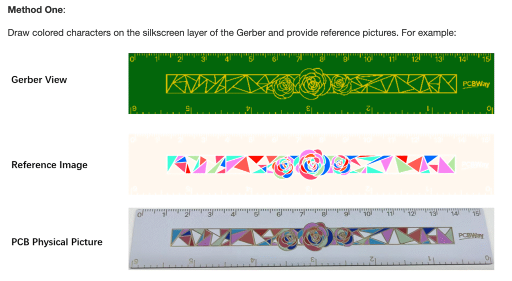
The first thing they contacted me about was the silkscreen layer on my board. In their instructions for the UV printing process they say “Draw colored characters on the silkscreen layer of the Gerber and provide reference pictures.“
I took this to mean, “put references on the silkscreen layer” and send us the image we should use. They contacted me asking a question. Did I want the silkscreen layer?
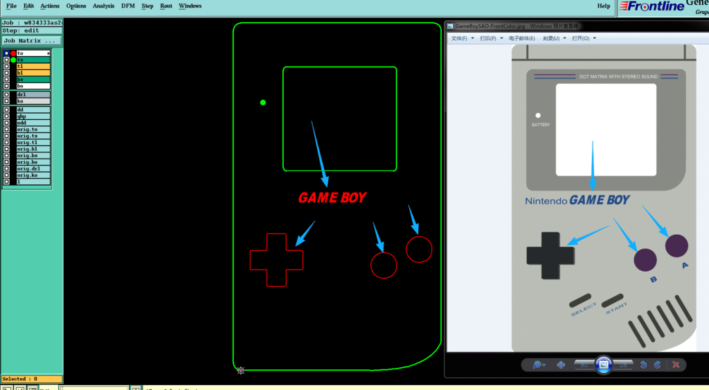
I didn’t of course, I wanted just the provided image. It was a bit more clear after the fact. I replied that I didn’t want that and they fixed it!
Printing proofs
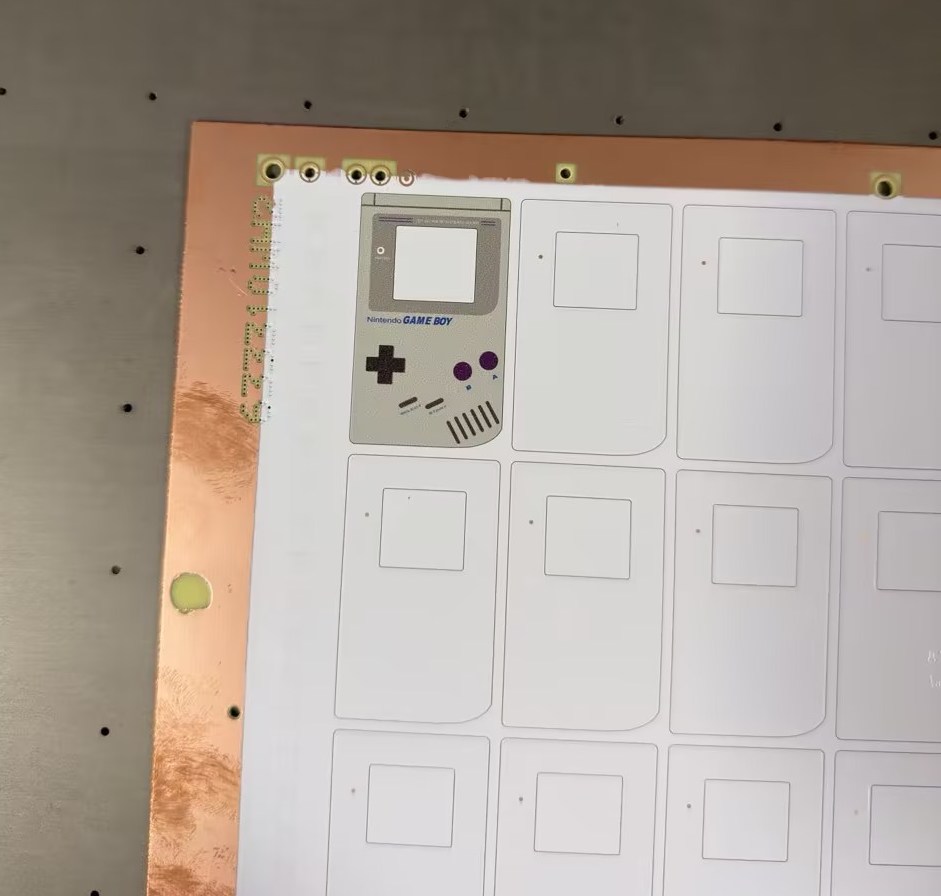
I don’t recall checking a box about getting a printing proof, but I got an email anyway asking about the printing. The printing on the left is the first attempt. It looks good (this image is scaled about 4x) but there is a gap around the “battery” indicator that I didn’t like. I assumed that there was a limitation in the printing process that was causing that. The indicator is meant to pass-through light from an LED on the other side. There’s no copper, soldermask or silkscreen between it and the LED – just the fiberglass substrate.
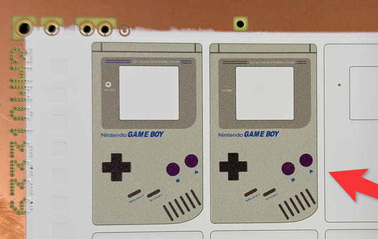
I asked if it was possible to print in that space, and my account contact sent a message to the engineers asking if they could do it. Much to my surprise, they came back with it fixed perfectly!
I’m hopeful that in just a few more days, these boards will be shipped to me. We’re definitely going to be down to the wire on this one!