
I had reached a stopping point with the keyboard board. I had reasonable design did everything I needed it to do – with one, kind of glaring oversight: The board didn’t fit in the iBook chassis.
This issue at hand is here:
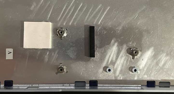
Between the 3 mounting posts on the chassis, there’s a piece of hard rubber that sits directly under the keyboard connector. I think it’s there really just for when the keyboard is plugged in – to keep the pressure from buckling the logic board too much.
Unfortunately, it’s in the way of the Pi Pico. This could be removed with some effort, and for my one-off project it probably wouldn’t be that big of a deal. But as I mentioned before, I’m not the only one going to be using this board and reducing the work otherwise is a net win.
Version 3
For this version of the board, I ditched the Pico in favor of laying out an RP2040 board myself. This is a solid design- provided that I routed everything correctly. In this design I used 0805 SMD components, and even those were annoyingly large relative to where they needed to be positioned.
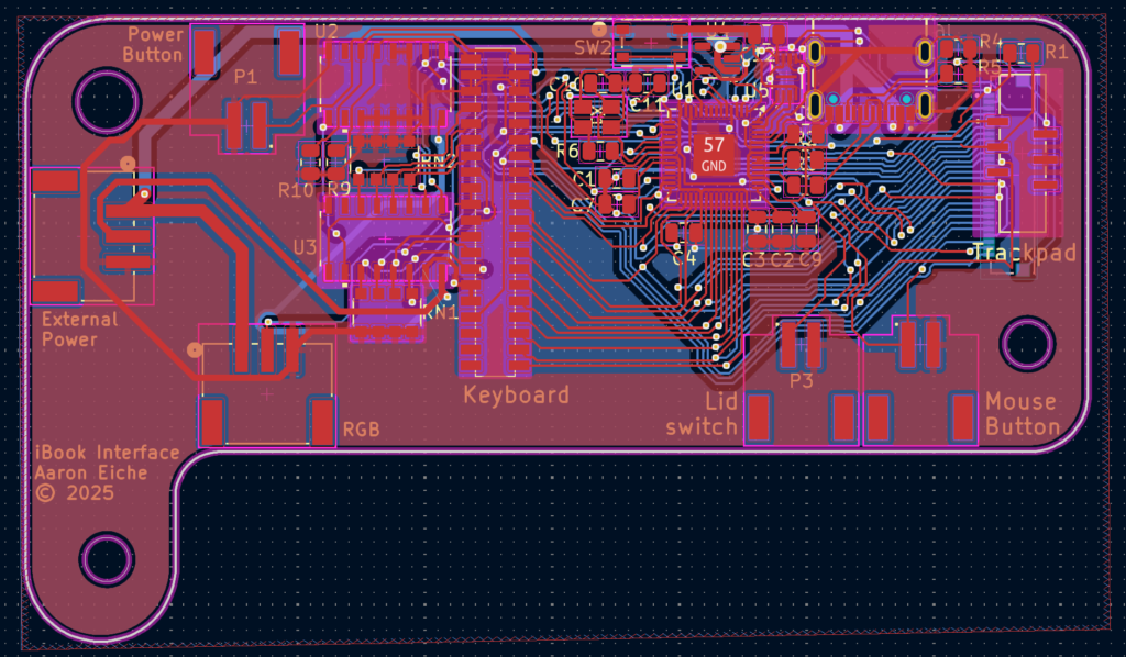
I was mostly done with this version, but looking back at it I realize this would not have worked as the power button connector would get in the way of the keyboard plug
Version 4
Two things drove this version:
- Someone in a forum mentioned that the cost of a 4-layer board wasn’t much more than 2-layers, and it vastly simplifies the layout.
- I gave up on the Pi500’s on-board rp2040 to drive the keyboard.
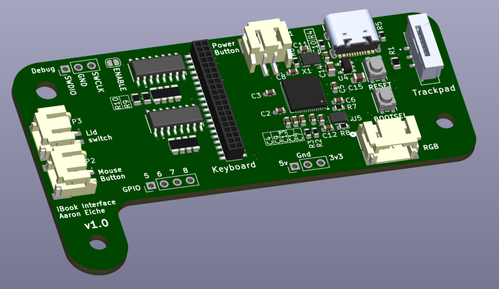
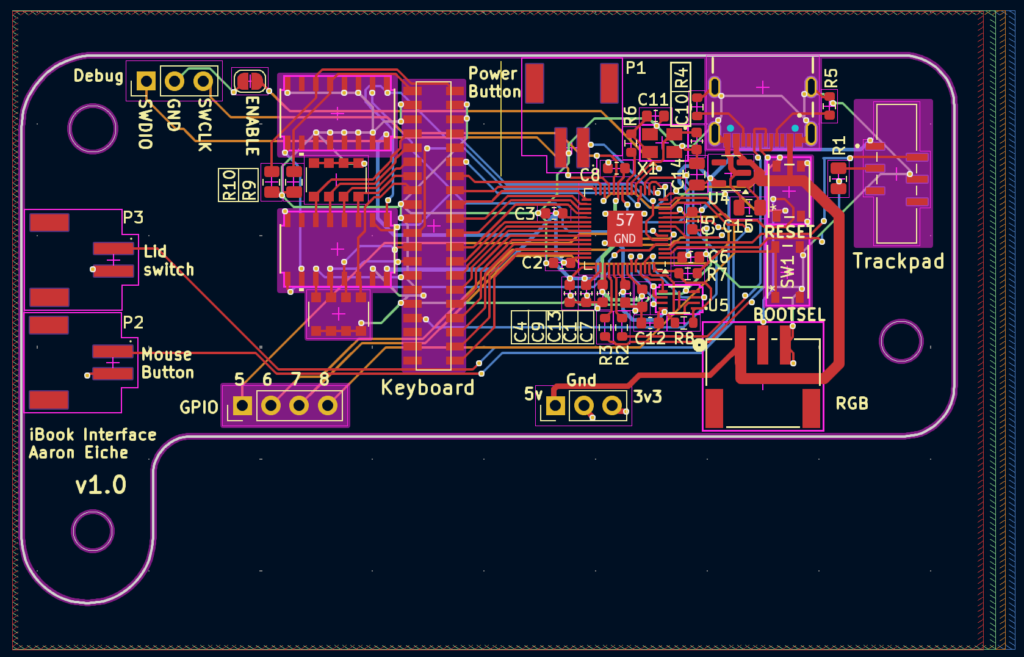
I really liked the idea of using the RP500’s on-board microcontroller for the keyboard. I found myself doing a lot of contortion to make it work. All-in-all, it wasn’t really saving me time or money (not much anyway) to make a special connector. So I decided to connect the board to USB internally, and ditch the 26 pin connector all together.
This design replaces the 0805s with 0603 components. They’re harder to place by hand, but can be placed closer to the chip – and solve some electrical challenges. This is also my first time laying out a 4-layer board. Initially I thought vias that were front-to-back meant that they didn’t connect to the inner layers. My board got rejected on its first attempt as the board house I’m using (JLC PCB) doesn’t do “blind” or ” buried” vias. I had to go back and correct them all.
Really the only downside I faced with the 4-layer board was that changing the color of the soldermask immediately increased the price by huge amounts. Sometimes 2-to-3 times the cost. Green isn’t very exciting, but it’s cheap.
If you look near the power button connector, you’ll see a yellow line. This is where the keyboard header comes out to, so I wanted to make sure I had plenty of clearance.
Lastly, this version gave me a chance to add in a few extra headers. Dropping the off-board connector meant I had 4 extra GPIO to expose (If I wanted), as well as break out the built-in debug pins.
One last note: This is obvious in hindsight, but if you’ve not made a bunch of circuits you might miss it. You schematic and PCB should go two ways. I found when I was laying things out that I had just set all the pins and was trying to route them according to my schematic. In a lot of cases, these were just GPIO and I could reassign them in any order or which-way I wanted. Don’t be afraid to adjust your schematic to accommodate your layout.
PCBs on the way
I have ordered this version of the board, and I expect to have it in a couple of weeks. I went for the slow shipping option because I’m not in a rush.
Next steps
Once I get the PCBs and the parts, I’ll assemble a couple and test them out. With any luck, I should have a working keyboard and trackpad setup! After that, I have to solve the thorny problem of the display.