I once asked in a Discord chat if I was missing something about KiCAD because I preferred to make board outlines and other design work in FreeCAD or Inkscape. The answer was that KiCAD’s tooling for that sort of work was pretty limited, and the recommendation from KiCAD devs was to do your board shapes in other tools and import it in.
This is how I’ve been approaching the StarSensor design. I started out in FreeCAD because it is the tool that I feel like I know the most in terms of sketching. I know how the tools work, Making the StarSensor isn’t just a matter of copying though. It’s reverse engineering.
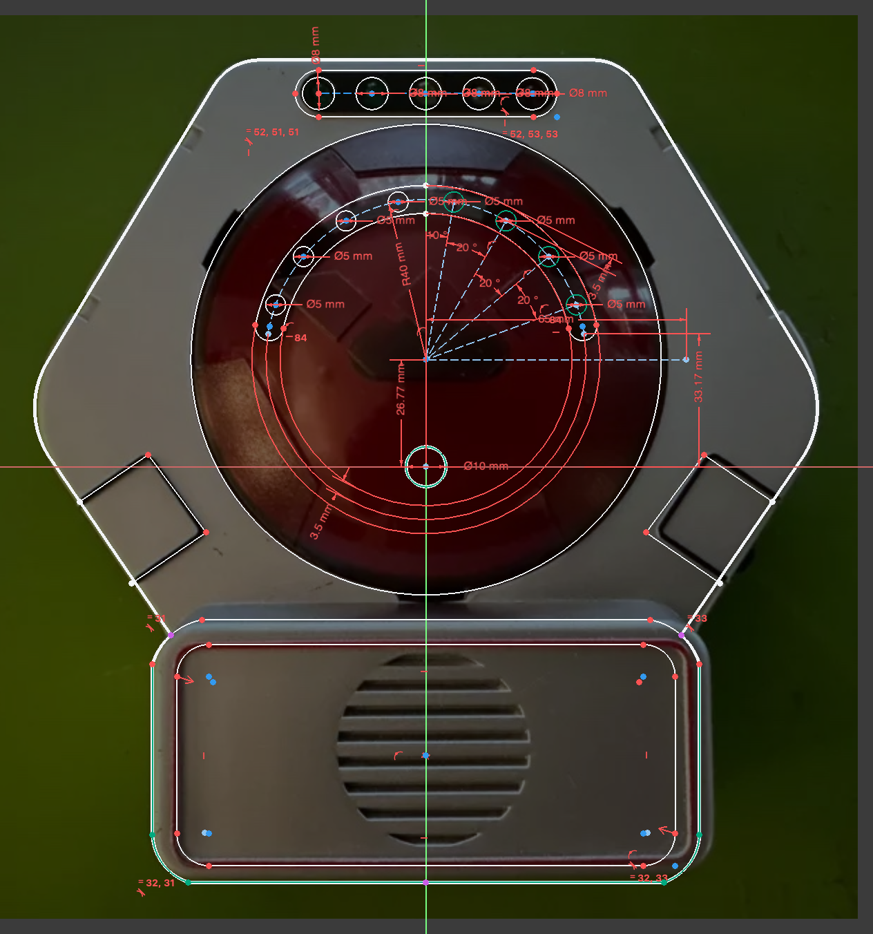
A lot of the drawing was capturing the gist of the StarSensor. Because of angles and the deflection of the lens of whomever took the pictures, this StarSensor is imperfect as a reference picture. So I did my best to trace around it. For a lot of the features, instead of introducing constraints I just found what I liked and mirrored the sketch elements. This makes it harder if I want to go back and change it, but quicker when I was just trying to get the shapes out.
Inkscape
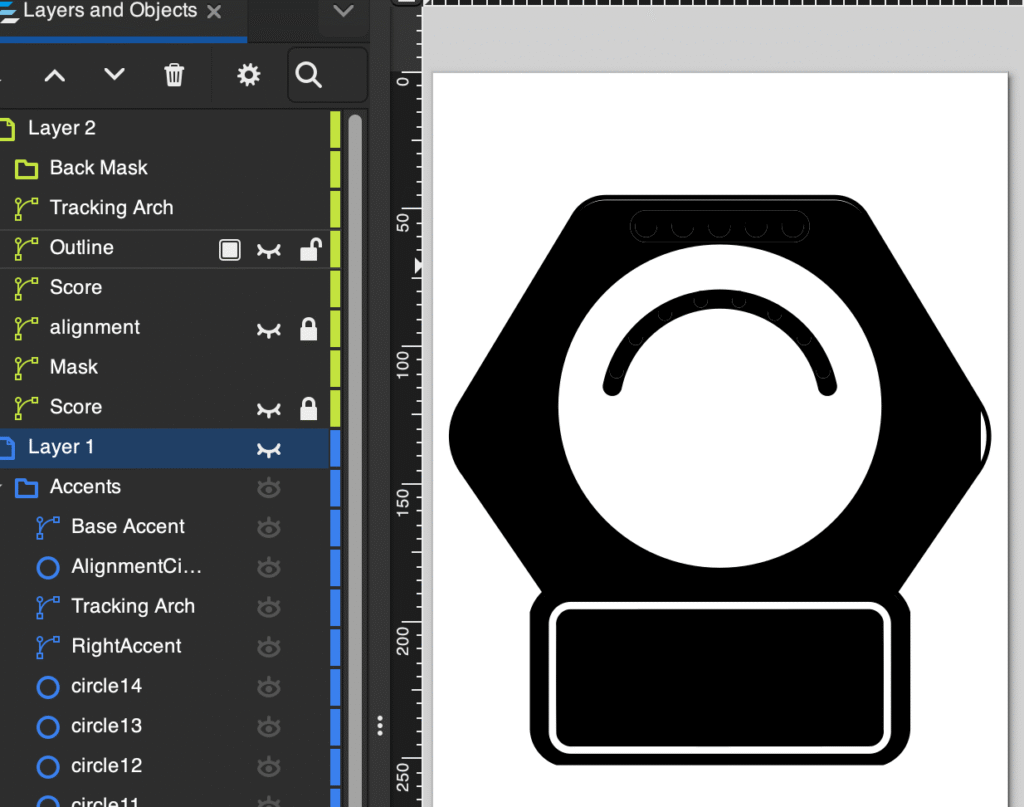
I probably could have achieved what I did in FreeCAD in Inkscape, but you use the tools you know. I brought the Sketch into Inkscape to start creating the various layers for KiCAD. This was a real learning process for me. Essentially I would make differences or unions of various shapes and then import those shapes into KiCAD. One technique I learned that really helped me was using the outline in every export. This made it really easy to align everything. You take the outline, and center vertically and center horizontally. You can then delete the extra outline you have leaving the graphics you want.
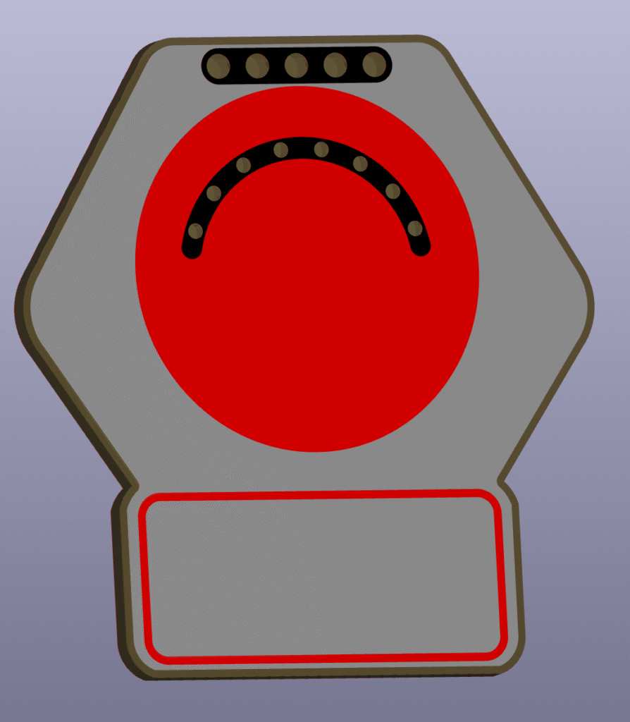
Once I had the technique down, the real challenge was figuring out how to get what I wanted. Mostly a matter of how the soldermask, the HASL finish, and the silkscreen would go on. In some cases, I needed to ensure the soldermask was where the silkscreen would be, as it wouldn’t properly bond on the HASL surface.
Electronics
I’ll cover this in a post in the future, but once I had the visual presentation more or less finished, I decided to get the hardware sorted as well. This is a rough layout, still leaving room for a piezo buzzer and maybe an action button.
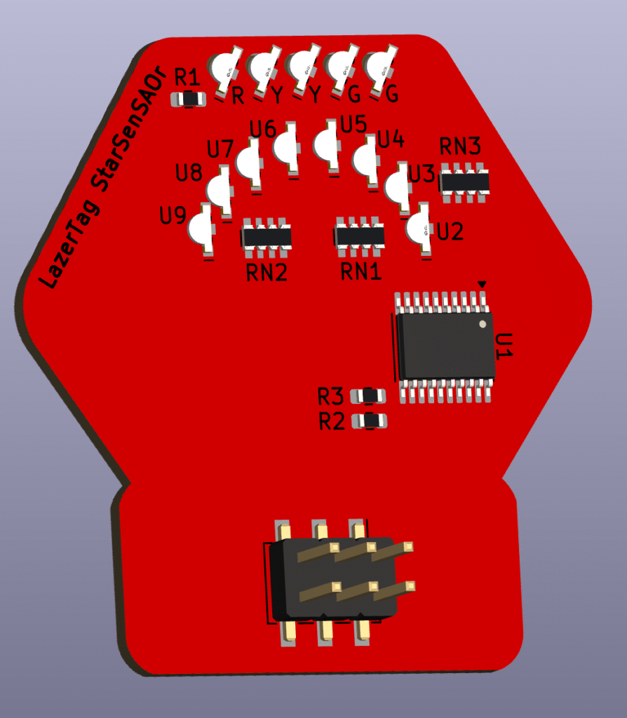
I’m really pleased with how it’s turned out so far. I’m thinking about how to handle the light bleed from the LEDs. The side-firing LEDs are positioned to shine right through the PCB substrate. But, the substrate itself acts as a bit of a light pipe and you can see the light coming out the in other spots. I’m concerned that the light will bleed between LEDs. One idea had (not sure if its feasible) is to put vias between the LEDs. The vias would be plated during production and make the space opaque(ish).
Anyway, the design is coming along!