 (This tutorial has gotten really popular recently, and I’m very pleased that so many people are interested. I learned all of this stuff while working on my first PCB. If you’re interested, I’ve started to sell the most recent version of my Arduino ProtoShield. If you’re making a shield, have fun and good luck!. If not, I hope you find something useful here -Aaron)
So you’re pretty fond of your Arduino. You make blinking lights, and beeping noises. You’ve made a robot that was pretty cool. Or maybe you didn’t. Who cares, You’re ready for the next step. You want to extend it. Although you can just plug in wires, there’s something very appealing about making a shield. Instead of a rats-nest of wires piled about and plugged into your prototyping breadboard, you can have a nice clean shield with labeled connections and a smaller footprint. So here I’m going to tell you everything you need to know to make a schematic and PCB layout, and get a beautiful shield that will plug into the top of your Arduino.
Specifics about this tutorial:
There are a couple of things you should know going into this. First, I’m not going to teach you everything about EAGLE. EAGLE is a complex program, and it’s pretty awesome. There’s no way I could cover it all. Second, this tutorial came about as a way of trying to get more people into my local PCB order. We try to fill up our panels so we can get one out every 2-4 weeks, and we recently had to switch production houses. As a result, this tutorial doesn’t have any info on etching your own PCB, just on getting the Gerber files out. So come check out our PCB order, because it’s awesome. Lastly, for the sake of simplification, we’re going to make a board that uses only parts in the SparkFun Library. This is because I don’t want to try to teach you how to make parts on top of everything else we’re going to be doing. It’ll just be easier this way, I promise. Okay, one more thing: I assume you know how to use your computer. This isn’t going to be a “how to use your mouse” tutorial. I’m gonna go with some things that are EAGLE specific, but you need to know basics. At this point, I’d be surprised to find someone who’s unfamiliar with computing, but has a strong enough interest in electronics to be to the point of designing their own PCB.
Things you will need:
You’re gonna need these things before you get started.
- An idea for your shield – I can’t help you with this one.
- A copy of CadSoft’s EAGLE program – for laying out your PCB
- A copy of the SparkFun EAGLE library – for the components.
- Your preferred Fab house’s Design Rules – Our PCB order rules are here.
- An EAGLE CAM job for separating out Gerber files. Here’s ours.
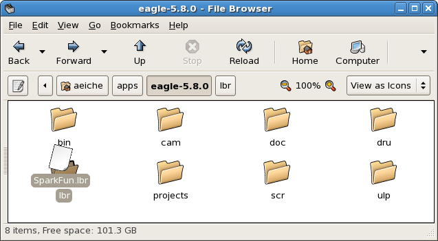
After you download and install EAGLE, download and extract the Sparkfun library. You should get a file called “Sparkfun.lbr”. This is an Eagle Library made by SparkFun Electronics. I like this library because it has a wide variety of components and reliable footprints. (Footprints are the measurements for parts that end up on your printed circuit board, and it is absolutely crucial that they’re correct.) One advantage of the SparkFun library is that everything in it licensed under the Creative Commons 3.0 Share-alike license. This means you can use it commercially, so long as you share any adaptations your create. Another library I highly recommend (but is not necessary for this tutorial) is Adafruit Industry’s Eagle Library.
Once you have the Sparkfun.lbr, copy it into the “lbr” directory in the directory EAGLE is installed in.
Let’s Make a Schematic:
I told you I couldn’t help you with your shield idea. That’s not entirely true. Since talking in the abstract all day is a pain the neck, we’re going to make a simple shield that does a few simple things. Our shield is going to light up lights, and connect to sensors.
First thing we need to do is make a new project. Open up EAGLE from wherever you installed it, and you should get a window that looks a little like this:
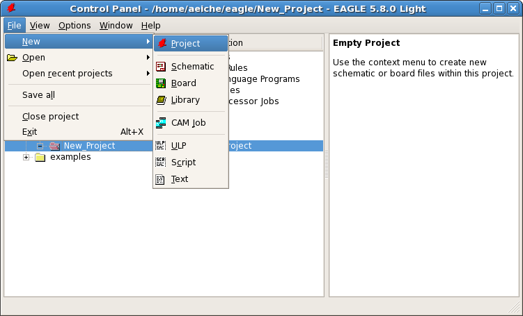
Click on the File menu, hover over new, and when the sub-menu pops up, choose “project”
You now should have a new project folder under the projects heading in the control panel window. Go ahead and give it a name – I chose “New Arduino Shield”, but you can do whatever you want. There won’t be anything in the project right now, so let’s add something. Select your new project folder, and then click on the file menu, go to ‘new’ and choose “schematic”.
You’ll get a window that looks like this:
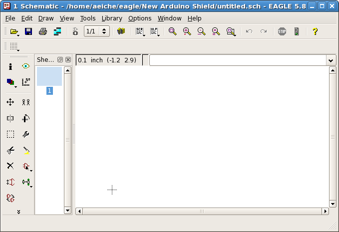
Your schematic is the blueprint for your circuit. It describes what is connected to what, and how. It does not describe what the PCB will look like. Don’t worry too much about how your schematic goes together. The important parts are to make sure the schematic layout is simple, and readable.
We need to get some parts in there. Namely, we’re going to want some terminal blocks, some LEDs and some resistors. First though, let’s add the Arduino pins themselves. You’ll want to select the “Add a Part” Button on the left hand side of the window. It looks a little like a plug with a pointer on it. It’s this one:

That will bring up a dialog called “ADD”. On the left-hand side of this window is a list of all the libraries that EAGLE has access to. The right-hand side shows information about the item in the left-hand side.
You’ll want to find the SparkFun item in the list. (As a side note, this list isn’t quite presented in alphabetical order. The methodology here puts all capital letters ahead of the lower-case ones. The list goes from A-Z, then from a-z.) Choose the SparkFun item, and click on the plus sign to expand it. If you don’t see any items in the left-hand side, go to the library menu and click on ‘use’. This will bring up a list of EAGLE libraries, and you can select the Sparkfun library.
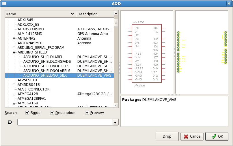
Scroll down until you find the item called “ARDUINO_SHIELD” and expand it. In here you’ll find a few different versions of the Arduino layout. Schematically, they’re all the same, but on the PCB side (in EAGLE parlance, this is called the “device”) there are a few different variations. You can click through the different shield options to see what the device footprint looks like. I prefer the ARDUINO_SHIELDNO_SLK, because I can worry about making my own board shape rather than relying on the Arduino shape.
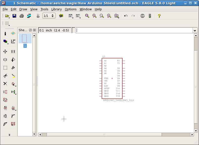
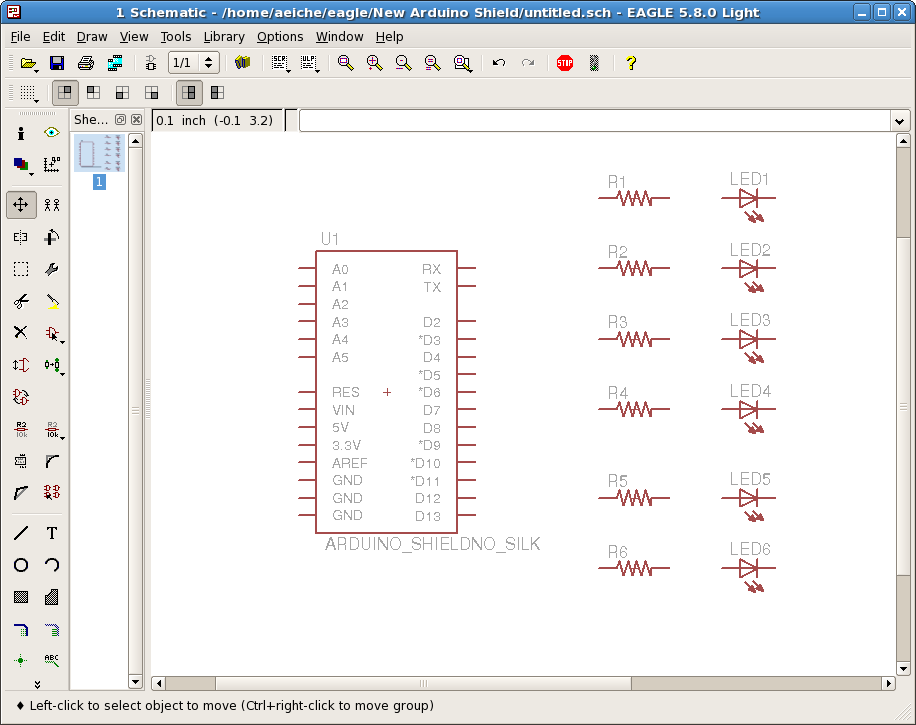
Once you click “Ok” the dialog will disappear and your pointer will have a schematic circuit attach to it (in EAGLE’s language, this is called the “Package”). Figure out a place to put it down and click your left mouse button. EAGLE will set down the package. You’ll still have a copy attached to your pointer, so hit ESC on your keyboard a couple of times to get to your window again. You should now have something that looks a little like this:
Click on the “add a part” button again, and this time, go hunting for a resistor. There is a sub-heading called “RESISTOR”. Under it, the most appropriate part is called “RESISTORPTH1”. When you click on it, the schematic package and the device footprint will be shown.
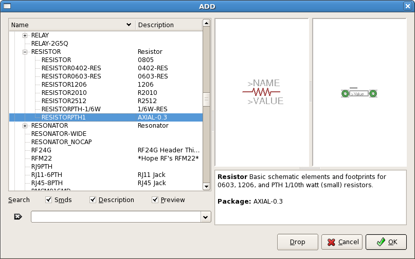
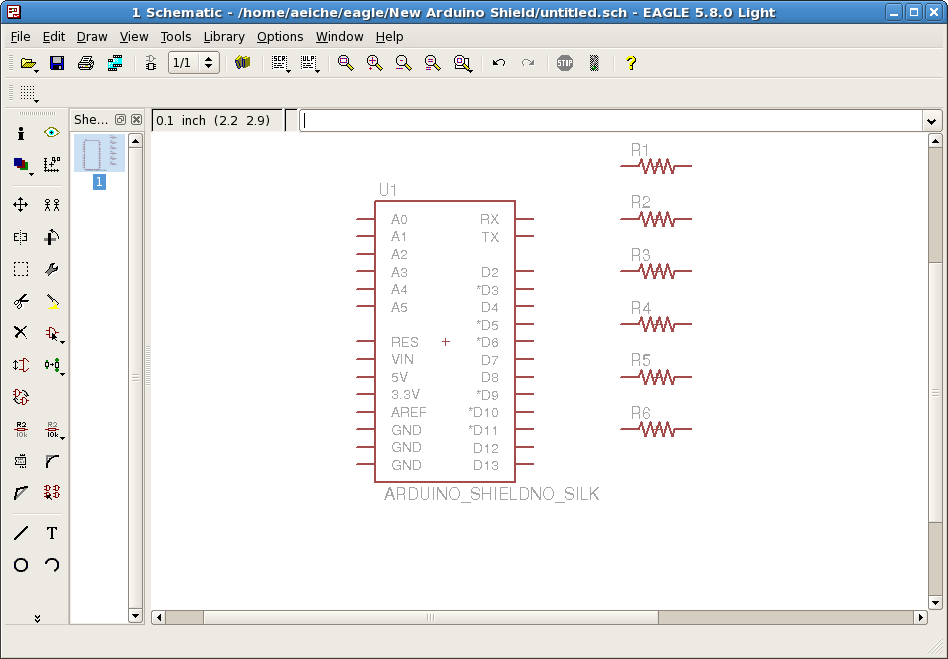
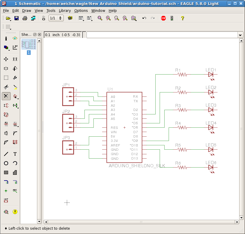
Click okay, and put down 6 of these guys. We’re going to put our LEDs on the PWM pins in the Arduino so we can control brightness (Note: You can actually pull off PWM on any pin on the Arduino, but it has to be done in software. We’re gonna ignore that for the moment.) Lay down the resistors just a little bit away from the Arduino package,
With the Resistors down, let’s put down some LEDs now. Click on the “Add a Part” button again and find the LED heading. In there, select the LED5MM Package, and click okay. Now you want to lay these out. It’s important that we put them the right direction. You can remember which side is which with a simple mnemonic device: A is for Anode. That is, the end of the LED with the arrow is the Anode. Another easy thing to remember is that the side with the line, is the Cathode. That line (|) turns sideways and becomes a negative symbol (-) or ground.
You should now have a schematic that looks something like this:
Now, for our shield we also want to throw in a way to easily connect some inputs, namely sensors. The easiest way (In my opinion) to do this non-permanently is to implement a terminal block. Terminal blocks are those things you can screw, clip, or lock wires into place. The connectors are conductive so pushing the wire in makes it part of the circuit. We’re going to add one terminal for each of the Analog inputs. Terminals come in blocks, and we’re going to use 3-point terminal blocks. Most often these come in 3.5mm pitch (3.5mm between the posts). Once again, click on the Add A Part button, and head on down to the “M”s
You’ll find under the M03 heading a series of parts that are 3-point connectors. We want the M03SCREW (Alternatively, if you want you can use the M03SCREW_LOCK – This is the same part, but the holes are just a tad wide apart. They make the part stay in place more easily when you flip the board to solder the pins.) As we have 6 analog pins, we’re going to put a pair of them on the schematic.
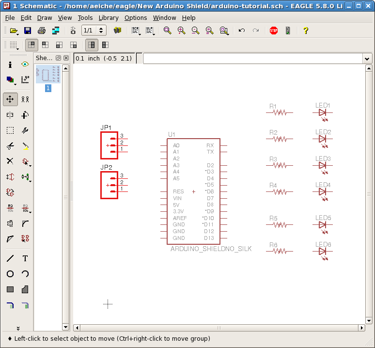
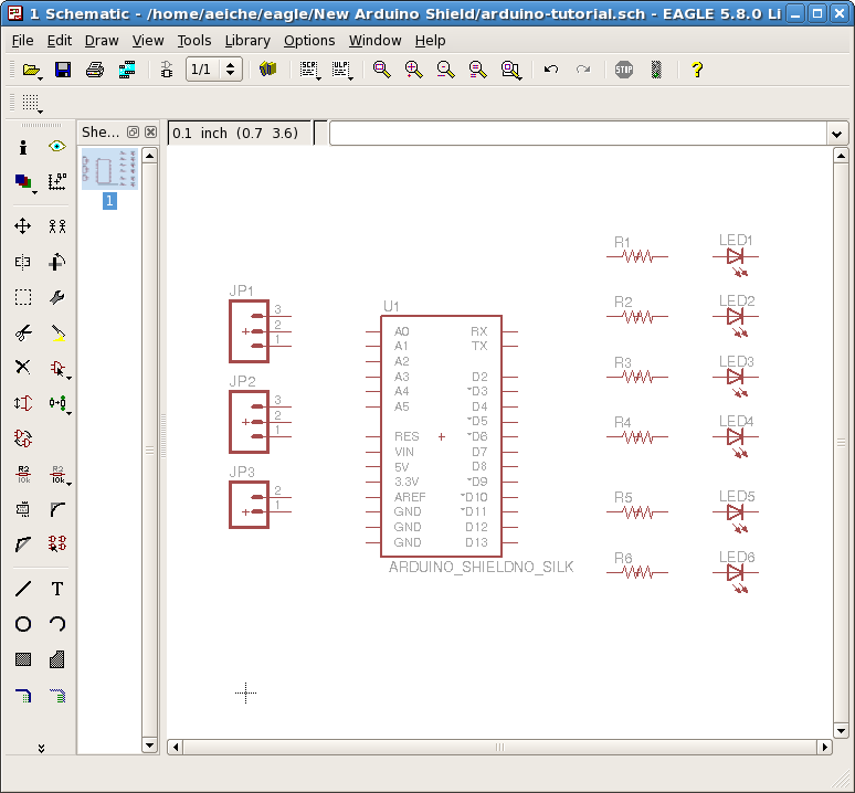
For the convenience, we’re going to throw in a power terminal. This will just give us screw access to the 5v line and the Gnd. A 2-point terminal block is a lot like the 3-point one we just added. It’s listed under the M02 heading in the SparkFun library, called M023.5MM. You’re an old-pro at this by now. Stick it in, and you should have something like this:
Okay, we finally have all the parts we want. Let’s wire up this thing!
You would think that you want to use the “wire” tool to draw connections between components. You do not. You want to use the “Net” button. The net button is a little tidier than the wire button, does things right, and makes everything better. The Net tool button looks like this:
![]()
Select it. (Even though it looks like it, it’s not grayed out. Also, don’t confuse it with the button immediately next to it called “Bus”) We want to draw lines between the PWM pins on the Arduino to the resistors. The PWM pins are marked by a small asterisk (*) on the chip. They are D3, D5, D6, D9, D10, and D11. When you click on the wire, it starts another segment. Start at the pin on the Arduino, and click. You should now be dragging a line. Click again to create another segment. When you’ve gotten to where you want to end, hit Esc, or Triple click. This will stop the line. Do this for all 6 PWN pins and you should have something like this:
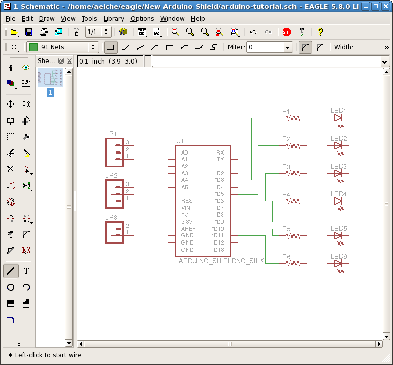
Now attach each resistor to it’s associated LED. You should now now have this:

Now let’s attach the terminal blocks. Everything should go in order, except for the power block. Because of the way the pins are setup on the device, we want to pull the bottom most ground pin from the Arduino and the 5v line. When you’re done, you should have something that looks like this:
We’re almost finished. We just need to complete our circuit to make everything work right. To do this, we need to run a ground line over to the LEDs. Grab the wire tool again and draw a line from the top GND line on the Arduino and carry it around to the side with the LEDs. Why the top GND line? Well, the way that the schematic translates to the board later, puts one of the GND pins on the side with the digital pins, while the other two are on the side with the analog pins. So this is for convenience.
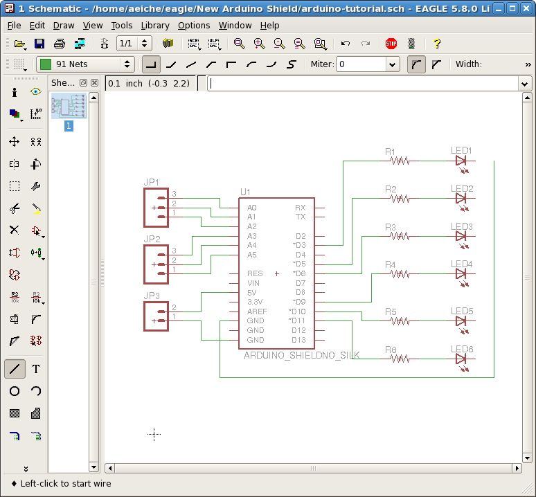
Now connect each LED to the ground line.
That’s it! We’re done with the Schematic and we can move onto producing the PCB. Be sure at this point (if you haven’t already) to save your schematic. You never know when something will go wrong and take away all your hard work. You may want to try laying out the whole thing over again, just for the sake of doing it. Going through the process a few times will really help you get a feeling for EAGLE’s quirks and the processes in it.
Making the Board:
Now the fun part! I call this the fun part because I enjoy the process of figuring out how to put together the circuit in a way that makes sense. With an Arduino Shield, there are a couple of things already solved for you: 1) You don’t really have to worry about Orientation, the shield is only going to plug in one way. 2) A lot of your layout is already fixed (This can be a mixed blessing though.)
At the top of the window, you’re going to see a button that has two things on it. The button is called the ‘board’ button (in the schematic window) It has a symbol on it that looks like a plug (actually, it looks like a AND gate, but if you’re not familiar with electronics schematics at that level, it’ll probably look like a two-pronged plug) The other symbol looks like a 6-pin IC. The button looks like this:
![]()
When you click on it, you will probably get a warning that looks like this:
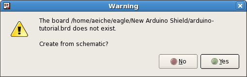
Click “yes” and it will open up a window like this:
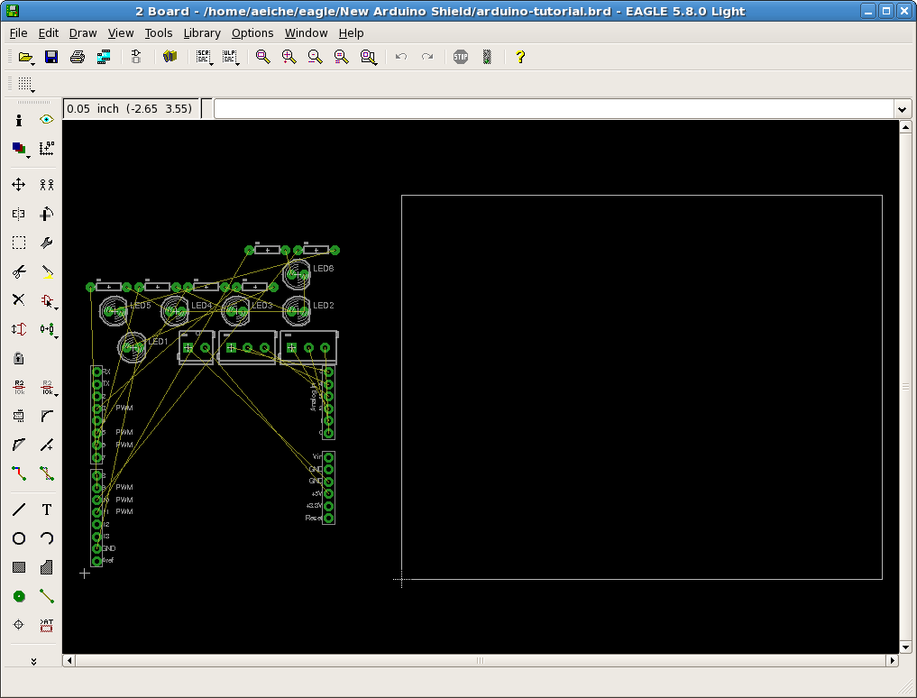
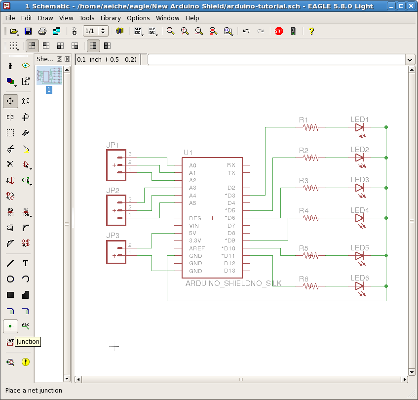
We need to move all of those parts into that white square. Click on the “group” tool (this is the dotted square)
![]()
And click and drag around all the parts.
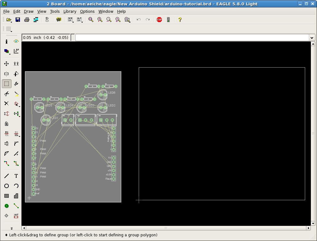
This should highlight all the parts. Now you need to click on the “move” button. It’s the one that looks like a cross with arrows on each end:
![]()
And right click on one of the parts. This will bring up a long list of items.
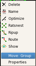
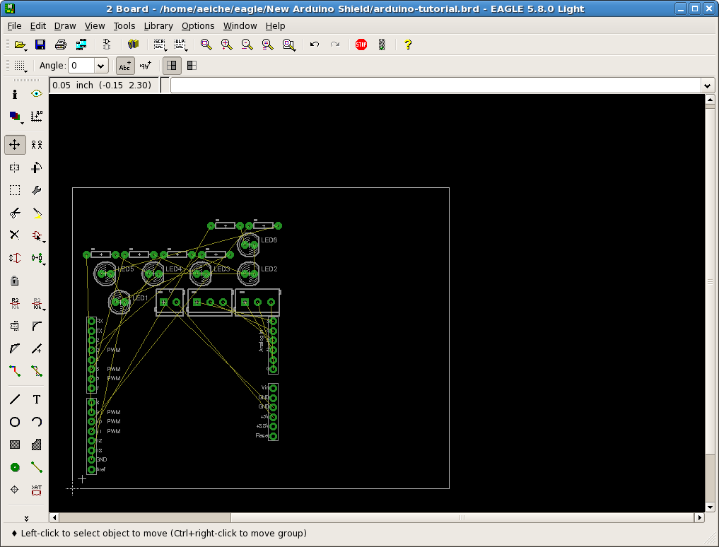
Click on “move group” should attach the whole group of components to your pointer. You want to move all of these things inside the white box. When you’ve done that, you should something something like this:
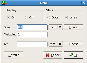
Before we continue, we’re going to turn on the grid. You don’t have to do this if you don’t want to, but when you get to more complex boards, you’re going to really want to use the grid. It is absolutely crucial in PCB design. To begin, click on the Grid button in the upper left hand corner:
![]()
This will bring up a dialog. You’re welcome to set it to whatever you like and you might want to mess around with it to get a feeling for what it can do. I like to work in 0.1 inches as it’s the most common header in the US. Additionally, there’s an ‘Alt’ setting which produces a secondary grid you can work with. I usually set it to 1mm because that’s a common measurement as well.
Once you click okay, you’ll get a space that looks like this:
If you don’t like the size of the grid, you can certainly change it. I’m going to turn off my grid because it can be a bit distracting. This doesn’t mean that the grid is actually gone, just that it’s not displayed. When I get to positioning the components, it can be useful to have. Do whatever works best for you.
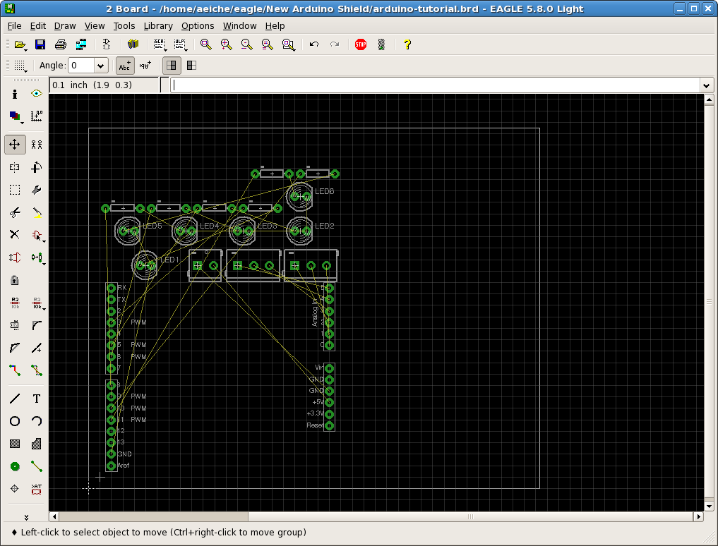
When I’m making an Arduino shield, I prefer to have it oriented the same way as the Arduino itself. That is, the top is viewed either as the side with the USB connector, or the side with the digital pins. For whatever reason, when SparkFun put together their Arduino component in EAGLE, they make the component default to a position with the digital pins on the left-hand side. In order to make it easier to work with, I rotate the whole thing. EAGLE makes this easy because whether it’s up or down, the names and values remain upright and readable. At this point, I’d tell you to use the rotate tool, but for whatever reason, I can’t get it to work properly here.
The method I use to rotate components is to choose the ‘move’ tool, click on the component, and then right click. As you right-click, the component you’re using will rotate counter-clockwise. So now you should have something that looks like this:
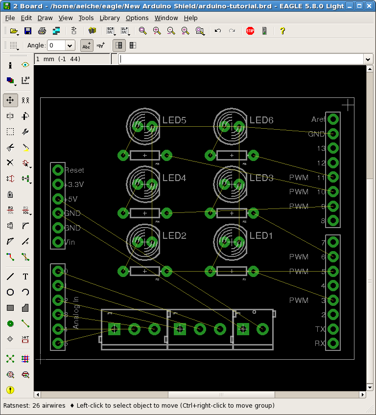
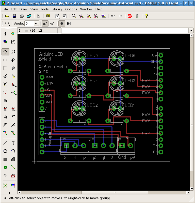
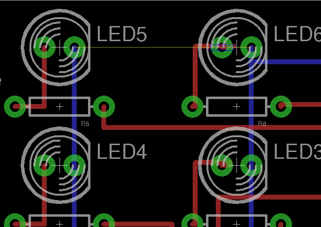
Now you’re going to want to begin placing components. This is largely up to you, and I’m not going to walk you through it step by step. You’ll see my solution below. Basically, move these components around until they make sense in their layout. The yellow lines (“air wires”) represent how the components are connected, and to what. The simpler the path is, the easier it will be to understand later. Try to keep them as straight forward as possible. Don’t worry if they overlap, that will all be solved in a moment.
See what I mean? Easy to read!
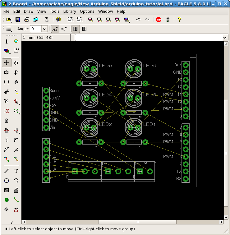
I should note here that most terminal blocks are designed to fit right up against each other, This is why I’ve placed the blocks so close. The particular ones that SparkFun sells actually interlock. You’ll want to make sure you properly line them up so the footprints are marked together. Because the footprints are tightly controlled, it can be a little difficult to position them correctly. These terminals IMO, are a little wonky, so here’s the simple solution: Put the 3-point terminals at 15mm and 26.6mm. I think there might be an error in the library with the 2-pin terminals. This image shows the block right next to the 3-pin terminal, but I don’t believe it will actually fit. If you choose to get this board produced, please fix the spacing or the part in the library.
You may want to resize your outline at this point as well. This is easy. Just take the corners of the outline and drag them to a size that works for you.
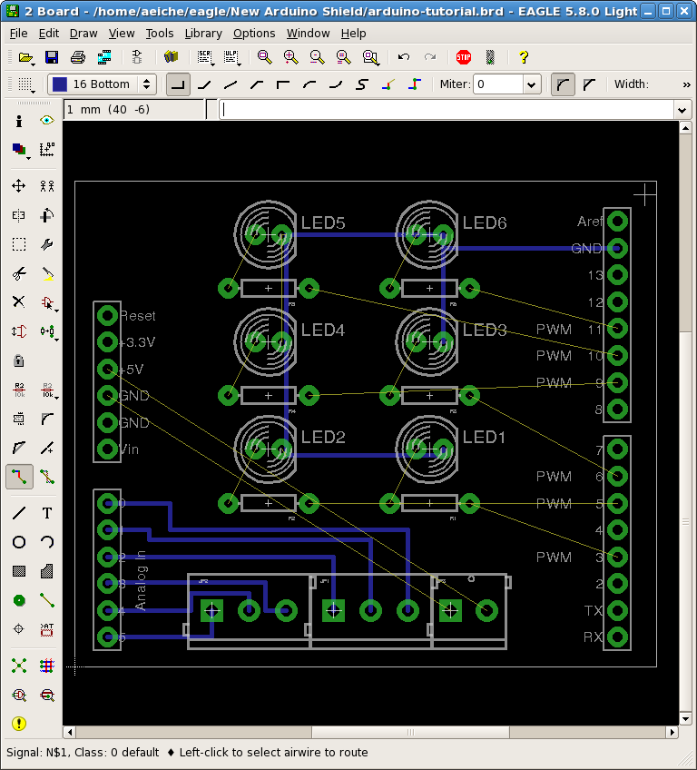
Now we want to take care of the routes. You could use the “Auto-route” button if you wanted to, but I prefer to do my trace-routing by hand. Because of that, it takes a little longer, but usually ends up neater in my opinion. First you’ll want to click on the “Ratsnest” button. This button takes all these little yellow lines that connect your circuit and moves them around to make things a little simpler.
![]()
Clicking that will recalculate the mess into this:
Now click on the Route Button
![]()
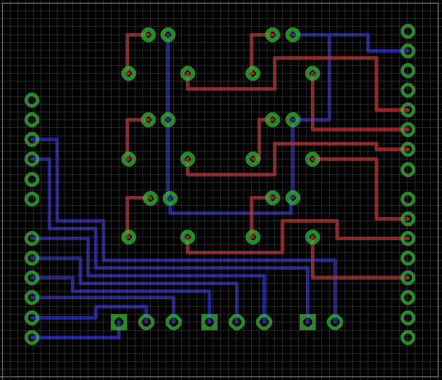
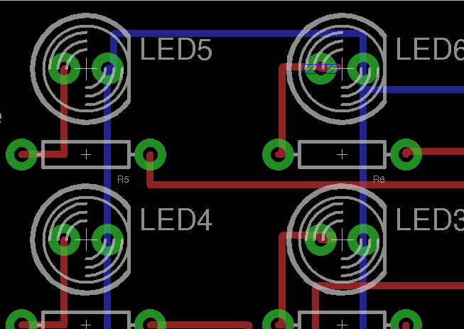
Now find one of the yellow airwires that connects to the ground line.Click on it, and you’ll start to draw a route. Don’t worry about crossing any of the yellow lines yet, we’ll take care of that in a minute. What you’ll find is that EAGLE automatically continues your line. As the LED’s ground line connects all of the LEDs together, we can just follow it around the board. Now let’s do it again with the lines coming from the 6 analog pins. Draw 6 lines with the route tool. You may have to get a little creative in how you draw the lines so they don’t connect with each other or other pads. Again, at this point don’t worry about crossing the yellow air wires just yet. When you’re done, you should have something like this.
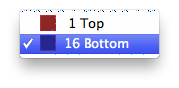
Okay. We’ve got 7 lines we still need to route, and space is getting pretty tight. What are we going to do? Fortunately, we have more than one side of the board to route on! In the upper left hand corner, when the route tool is selected, you’ll see a drop down menu. Currently it should say “Bottom” (meaning the bottom of the board) but if you click on it, you are able to select “Top”
You have to be a little careful because there’s less room on the top for routing than on the bottom, but with some creativity you can make it work. I recommend you take advantage of the gaps created by the resistors to take a route over to the other side.
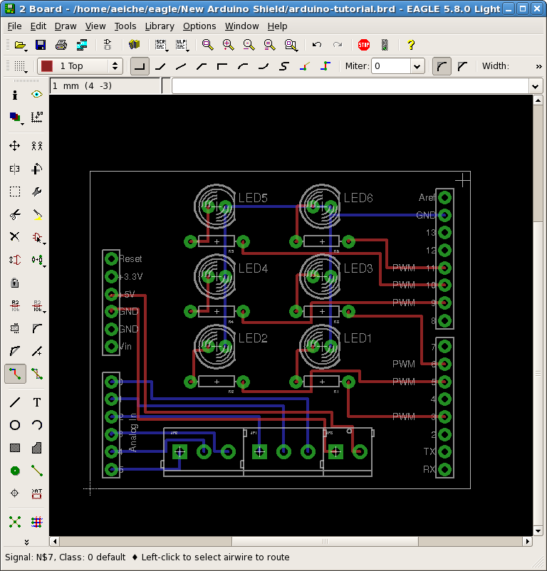
If it’s kind of hard to see, here’s a picture without the text that make show the routes a little better.
Okay. We’re almost done. We want to put a couple of things on the silkscreen, so we know what to plug in to the terminal blocks. This part is easy. Click on the Text button (The “T”). Type what you want, and place it. By hitting escape, you’ll get the dialog box again, and you’ll be able to place another thing. You might also want to fill in any blank space you have (or not) I like to put in something identifying, just for fun.
So here we are. We have completed our circuit and we’re ready to go! We’re almost finished (again). All we have to do is turn this sucker into Gerber files and shoot them off to the fab house.
Gerber? Isn’t that baby food?
Yup, Gerber is a brand of baby food, but it’s also the common name of the files you send to a manufacturer so they know what to do to make your board. It was initially created by a company called Gerber Systems Corporation. They used it to drive a photo-plotter. These days it’s properly referred to as RS-274X. There are lots of different “layers” in a gerber file, but the common ones you come across are as follows:
- Top-Silkscreen – This usually shows your documentation… part placement and footprints
- Mask Top – This shows the machine where not to put soldermask, like the pads you’ll be soldering onto
- Mask Bottom – Same as above, for the reverse.
- Top Copper – This shows where the machine should leave copper so your circuit connects
- Bottom Copper – Same as above for the other side.
- Excellon Drill – This is the file that tells the router where to go through your PCB
- Outline – Your board outline.
Allright, enough talk. Let’s do this.
First we need to run electrical and design checks. These make sure that nothing is electrically wrong with our design and that our fab house can actually produce it. Note: This doesn’t mean your design will work. It only means that EAGLE doesn’t see electric circuits crossing paths.
Click on the electrical check tool:
![]()
and it should bring up the ERC errors page. In this page there are a lot of warnings. Here it’s just telling us that there aren’t any values listed. I intentionally did that because I figured that someone may want to put their components. Who knows how big or how bright you want those LEDs. I’m not gonna tie you down. 🙂
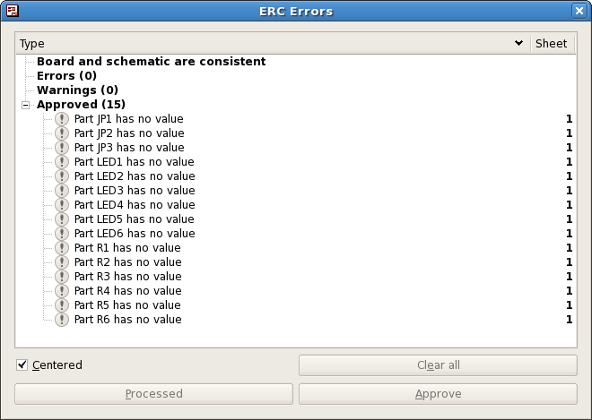
The way we take care of these is simply click on “Approve” for each one. Be careful how you do this, you don’t want to approve something that is wrong.
![]()
Next we’ll run the design rule check. Click on the design rule button
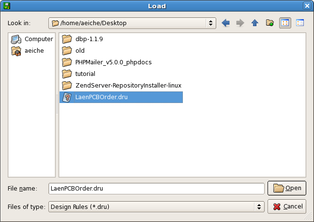
Since EAGLE doesn’t know who’s rules you want to play by, you’ll have to choose a design rule file, or a .dru. I use our PCB order rules, which can be downloaded at the top. Click on the “Load” button, and choose your file.
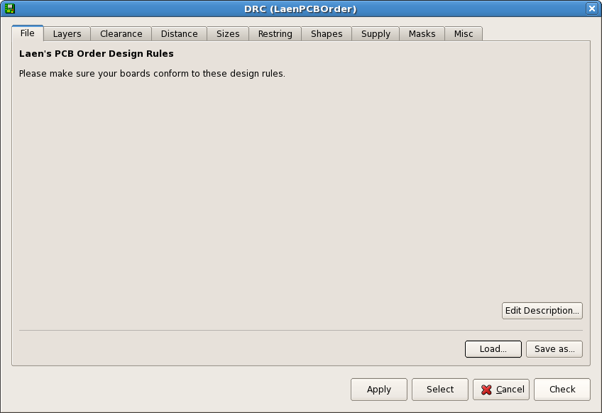
You’ll get the design rule check screen. Just press the “check” button.
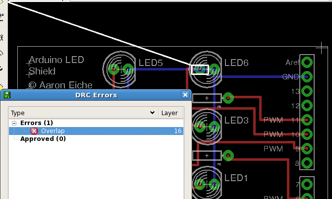
Uh-oh. Looks like I wasn’t paying close enough attention. There’s an overlap in the circuit layout. That is to say that something on my board is connecting in a way that is not connected on my schematic. Fortunately you don’t have to hunt around for it. EAGLE draws a nice little box around the area in question.
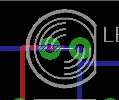
In this case, it looks like I ran my GND line right through one of the holes where the VCC line comes in. The way we fix this is “rip-up” the line and redraw it. The Rip-up tool looks like this:
![]()
All you have to do is click on the offending line, and then select the routing tool again an lay it down in a functional manner.
Okay, now that we’ve fixed that, we run the Design rule check again…
And it comes back good! Hooray!
Now we can finally produce those Gerber files. click on the CAM processor button
![]()
and it will open up the CAM processor Window (funny how that works.) We want to use a specific CAM job, so we have to go to File->Open->Job…
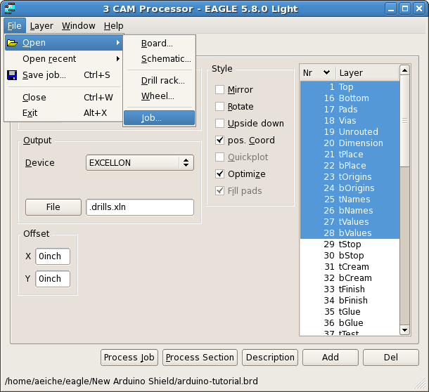
Choose your cam job, and you should get an updated CAM processor window:
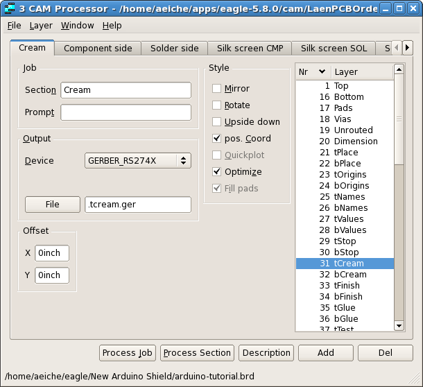
The only adjustment I recommend here is that you additionally select tDocu-51 on the Silkscreen-CMP layer. This will make sure that the Arduino Silkscreen stuff ends up in the silkscreen with the rest of our materials. When you’re ready, press the “Process Job” button. EAGLE will output the gerber files and output them into your project directory. EAGLE will have produced both .ger files and .gpi files. The gpi files simply contain information about the ger files, and are unnecessary.
If you want, you can see what these files look like by going over to circuitpeople.com and loading them up. It’s nice and simple. No signups, no ads. Just an easy way to view your gerbers. I highly recommend you do check your work to make sure it looks the way you want it to. I have gotten back boards that didn’t have everything on the silkscreen layer that I expected them to. Here’s how a couple of the gerbers looked from this project. On the left is the top-copper gerber, and the right is the top-silkscreen.


That’s it! You’re finished. Zip ’em up and send them off to your board house, or if you want it to be easy for yourself. Send them off to Laen, and he’ll include them in our monthly PCB order! I guarantee you, it’s hard to beat $5/sq in. for 3 boards. The turn around time is a little more than a week from send off date. And they don’t go out to China. (Judge for yourselves if that’s a good thing. I can go either way.)
If you’d like to look at the files I made while doing this, they are on the download page.
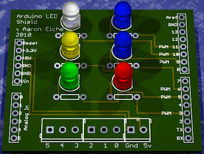
So there you have it. Make a circuit, order it, and in about a week-and-a-half, you get something that looks like this. If you need some help, you can usually find me during the week as sircastor on IRC on the #dorkbot channel or you can email me!
Hello Aaron
Thank you for this informative and detailed post – you must have read my mind, as lately I have been thinking about making my own shields as well. Congratulations for your efforts, and thank you once more!
Cheers
John